Using Atomic Layer Deposition to Protect Complex Geometries

The layered detail of ALD…

Atomic Layer Deposition (“ALD”), a method of thin film deposition, has become popular due to its ability to create a durable surface with high levels of control over thickness, composition, and conformality. Although the method has been around for decades, the more recent need to coat increasingly complex 3D surfaces has intensified interest in ALD.

Take a look at Shakeel’s ALD Deposition video for an in-person deep dive.

A subset of Chemical Vapor Deposition (“CVD”), ALD relies on surface chemistry that occurs between a solid substrate and gas phase reactant (called a precursor) using a process of sequential gas phase deposition cycles.

There are at least five specific methodologies, but generally speaking, there are two precursors that are allowed to react one at a time with a metal surface.  In this way, ALD differs from CVD because the precursors are never in the chamber at the same time.

And if you really want to geek out on this stuff, check out this amazing precursor database.

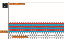
Repeated cycles build the thin film. The adsorbed precursor is held to the substrate by chemical bonds, and so the chemical process is self-limiting due to the constraint of available substrate atoms; the reaction is over once the substrate surface is saturated.

This is the key to uniformity and control over thickness, conformality, and composition.

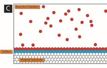
The following schematic gives a nice picture of how this works.

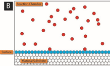
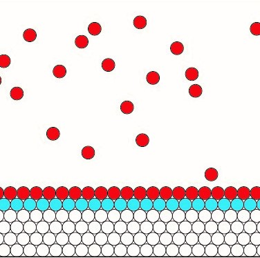
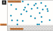
In panel A, precursor 1 (blue) is added to the reaction chamber containing the material surface to be coated by ALD. After precursor 1 has adsorbed on the surface, any excess is removed from the reaction chamber.

Precursor 2 (red) is added and reacts with precursor 1 to create another layer on the surface.
Precursor 2 is then cleared from the reaction chamber.
This process is repeated until a desired thickness is achieved and the resulting product resembles panel D.

Credit to: By Mcat chem446 – Own work, CC BY-SA 3.0, https://commons.wikimedia.org/w/index.php?curid=33220420

ALD has both industrial and research applications.

Most commonly, ALD has been used to grow oxides, nitrides, sulfides, and pure elements.

A familiar example is using trimethyl aluminum (TMA) and water to create a film of aluminum oxide, a high-k dielectric, and one of our specialties.

ALD has a slower deposition rate than other processes, and thus while highly suited for microelectronics and nanotechnology is not optimal for fragile or impure substrates.

Additionally, the precursors must be volatile but not prone to decomposition. Even so, the ability to use lower temperature during the process can benefit organic and biological substrates, and new ALD technologies that can be applied in the medical or biological industries are in demand and developing rapidly.

Another area in which we are seeing increased use of ALD technology is in the additive manufacturing space.  One of the benefits of additive manufacturing is the ability to produce complex shapes in one print cycle, made from a variety of substrates. 

However, these complex geometries are difficult to coat with a protective barrier using technologies such as physical vapor deposition (PVD), which is a “line of sight” technology. 

Atomic Layer Deposition is one of the best solutions to this problem.

With an increasing need for durable surfaces with chemical resistance, and a trend toward smaller devices with complex shapes, Atomic Layer Deposition has a lot to offer.

Shoot us an email or give us a call to discuss your complex shape.

We’ve got a coating that fits

image-7
Stay ahead of your big-brained colleagues and teach them about the latest coating technologies.
Loading